The U.S. Department of Commerce and TSMC Arizona have signed a non-binding preliminary memorandum of terms (PMT) for up to US$6.6 billion.
Takeaway points
- The U.S. Department of Commerce and TSMC Arizona have signed a non-binding preliminary memorandum of terms (PMT) for up to US$6.6 billion.
- The company also reveals its plan to set up a third fab at TSMC Arizona.
- Arizona’s three fabs are expected to create approximately 6,000 direct high-tech, high-wage jobs and 20,000 construction jobs.
What did TSMC sign with USDOC?
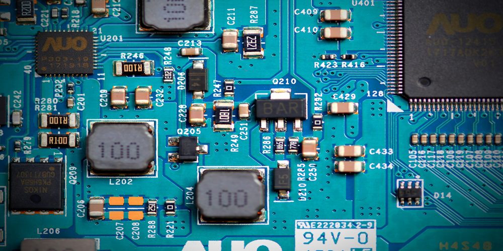
TSMC, a semiconductor manufacturing company, announced on Monday that it has signed a non-binding preliminary memorandum of terms (PMT) with the U.S. Department of Commerce for up to US$6.6 billion in direct funding under the CHIPS and Science Act. The company also reveals its plan to set up a third fab at TSMC Arizona. The aim of setting up the third fab is to take advantage of the most advanced semiconductor process technology in the United States to meet strong customer demand.
Based on the report, the company makes progress in completing its first fab and continues construction of its second fab at its Arizona subsidiary. Setting up the third fab brings TSMC’s total capital expenditure for the Phoenix, Arizona site to more than US$65 billion, making the site the largest foreign direct investment in Arizona history, and the largest foreign direct investment in a greenfield project in U.S. history.
TSMC Chairman Dr. Mark Liu said that the CHIPS and Science Act provides them the opportunity to offer services to the most advanced manufacturing technologies in the United States.
“The CHIPS and Science Act provides TSMC the opportunity to make this unprecedented investment and to offer our foundry service of the most advanced manufacturing technologies in the United States. Our U.S. operations allow us to better support our U.S. customers, which include several of the world’s leading technology companies. Our U.S. operations will also expand our capability to trailblaze future advancements in semiconductor technology,” Liu said.
Dr. C.C. Wei, the CEO of TSMC, said, “We are honored to support our customers who have been pioneers in mobile, artificial intelligence and high-performance computing, whether in chip design, hardware systems or software, algorithms, and large language models. They are the innovators driving demand for the most advanced silicon that TSMC can provide. As their foundry partner, we will help them unleash their innovations by increasing capacity for leading-edge technology through TSMC Arizona. We are thrilled by the progress of our Arizona site to date and are committed to its long-term success,” said Wei.
The Three Fabs
The company said that the Arizona’s three fabs are expected to create approximately 6,000 direct high-tech, high-wage jobs and 20,000 construction jobs.
According to the report, in the first half of 2025, the company will begin production leveraging 4nm technology. The second fab will produce the world’s most advanced 2nm process technology with next-generation nanosheet transistors in addition to the previously announced 3nm technology, with production beginning in 2028. The third fab will produce chips using 2nm or more advanced processes, with production beginning by the end of the decade.
Apple CEO Tim Cook said in a statement that “TSMC is at the leading edge of advanced semiconductor technology — and when that expertise is paired with the ingenuity of American workers, incredible things are possible. We are proud to play a key part in the expansion of TSMC’s U.S. production, and we’ll continue to invest in America and support a new era of American advanced manufacturing.”
In addition to the proposed US$6.6 billion in direct funding, the PMT also proposes to provide TSMC with up to US$5 billion in loans. TSMC plans to apply for U.S. Treasury Department Investment Tax Credits of up to 25% of the qualified capital expenditure at TSMC Arizona.